I tried to solder a hwfly / picofly onto my Switch Lite mainboard. Thanks to @Calvin I tried to work with leaded solder today and I think my soldering looks much improved now. However, there still seems to be something wrong.
My Switch always boots straight into the original firmware and I get the following error code on the Chip: blue (long) - pause - yellow - yellow - pause - yellow - yellow - pause - yellow - yellow
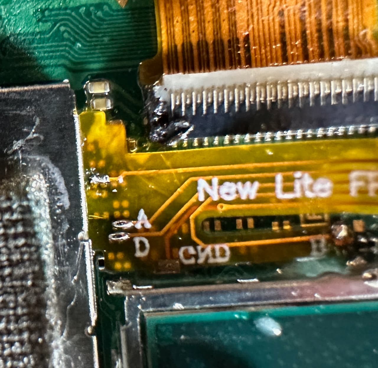
As far as I’ve read this has to be a problem with DAT0?
I already tried resoldering the DAT0 point several times, with no success. Am I missing something else? The thing is, I am very(!) afraid to destory the DAT0 solder points. I am already working on my 2nd mainboard because I ripped of my A solder points on the first. I really tried to improve my skills in the meantime, but maybe I am still not there?
Could somebody judge my work based on these smarphone pictures and maybe give me a hint what I could do?
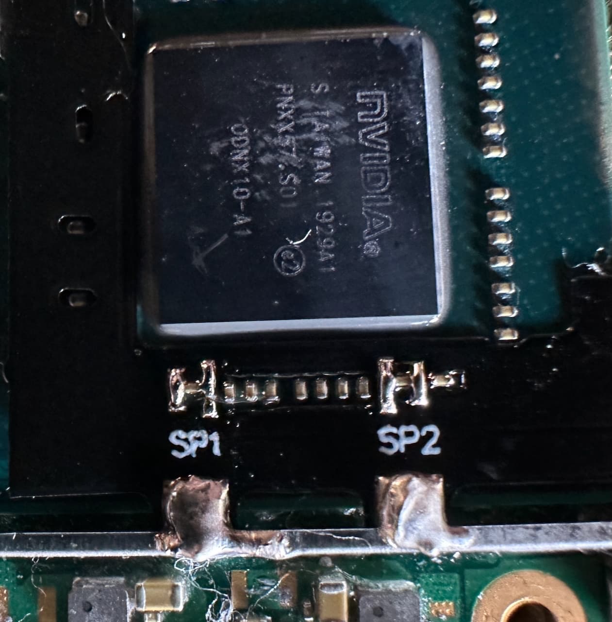
The second pic demonstrates the differences between leaded and lead-free solder: I tried to resolder SP1 and SP2 with leaded solder. The ground connections are from my earlies tries with lead-free solder.
I also already tried to solder a wire on top of the flexcable and directly connect it to C on the chip, same story. Next thing I would try is to try to get below the flexcable to directly connect to the C points on the mainboard and connect it to the chip, but I am hesitating since I really don’t want to make things worse.
Do I have to reassemble the Switch completely before testing?
The cartridge slot is not connected at the moment, just to rule that out as the source of the error.
It is maybe the angle, but it seems that the flex is a bit upwards.
I would pretin the pads and then lay the ribbon on top. With this newer version of the ribbon flex there are two holes in the connection pad and you can apply solder on the ribbon flex pads and push the ribbon flex on the pad beneath. With tweezers I would hold the ribbon flex down while removing the solder iron.
It is not necessary to full reassemble the Switch for testing.
I too have noticed that the C is a bit upwards, but since the A and D connections looked so nice I was very hesitant to desolder them.
Any tips on how to best get the flexcable loose again without running the risk of damaging the pins on the mainboard? I’ve read that using wick might lead to ripping them off the board, and I’ve had enough of destroyed pins with the first mainboard I tried to solder a chip to.
You can lift the ribbon a tiny bit with tweezers and put the soldering iron on C. When solder is liquid pull the flex a bit up, without ripping A and D. At A and D place the iron so that both get liquid at the same time and pull the ribbon flex up.
I am happy to report that I followed your advice and it worked great!
I will now try to practice a bit more with a different tip, as the one I was using just didn’t seem to work well with the small pads that are points A, B and C. I will then try to pre-solder the pads, this time with leaded solder, then clean the flexcable from the existing solder and at last try the whole procedure again. I will report how it went.
As promised, I am back to report my status. Took a while for the new soldering tips and leaded solder to arrive. I gave it another shot today and well… I am disappointed with myself.
At first everything went really great! Lacking a decent microscope, my strategy was to pre-solder more or less all the points and then attach the flex cable to A, C, D and B. It all seemed to work really great and I think I was able to align it well this time. However, after completing the installation, the Switch would no longer turn on. I desoldered the flex cable again, no luck. I then checked for shorts and found none. I also compared the mainboard with my old, now “donor” board and noticed that when pre-soldering I must have desoldered a resistor between DAT0 and the ribbon cable connector north of it. It’s definitely missing. One can see the part still attached in the first picture above, directly to the left of the (slightly burned part of the) connector.
I think it’s time for me to admit defeat.
I neither have the skill nor the equipment to properly do this, and I am a bit reluctant to invest into yet another board. I was thinking of desoldering the transistor with my heat gun from the “donor board” and transfer it, but without any decent means of magnification and proper tweezers (I don’t really trust my flimsy cheap ones) I think I’m out of luck.
Anybody lcoated in Europe that is willing to try to repair this if I sent the two mainboards?
Or should I rather write off the money and file it under lessons learned?